

This article originally appeared in USENIX ;login: magazine, shepherded by Rik Farrow.
As AI models grow larger and more complex, traditional computing architectures are hitting performance and efficiency limits. A new class of hardware, wafer-scale AI chips, pushes these boundaries by integrating hundreds of thousands of cores and massive on-chip memory onto a single wafer. Yet hardware alone is not enough: system software must evolve to fully harness its capabilities.
This article examines how the pursuit of AI scaling laws has led to the emergence of wafer-scale systems. We introduce PLMR, a conceptual model that captures their key architectural traits, and explain why today’s AI software stacks fall short in exploiting them. We argue that wafer-scale systems offer a promising path toward efficient scaling of test-time compute, mitigating the off-chip communication bottlenecks inherent in today’s multi-chip designs.
We then present WaferLLM, a system that achieves sub-millisecond-per-token inference latency, demonstrating how wafer-scale integration can deliver tangible scaling efficiency. We conclude with directions for rethinking the AI system stack in the era of wafer-scale computing.
AI scaling laws and the case for wafer-scale compute
AI scaling laws reveal a consistent pattern: larger models and more compute often yield predictable accuracy gains and emergent capabilities [1]. These trends point toward a shared goal, pursuing extreme computational scale and efficiency, underpinned by the expectation that progress toward AGI will require increasingly powerful systems.
The pursuit of scaling laws motivates the push toward larger AI chips. These chips integrate more cores and memory, with efficient on-chip communication to support intensive workloads. Larger integration improves efficiency by reducing costly off-chip communication, since more data can be stored and processed locally. This progression is evident in the adoption of chiplet and system-on-wafer technologies by AMD, NVIDIA, Google, and others, who continue to expand chip size across generations, as illustrated in Figure 1.
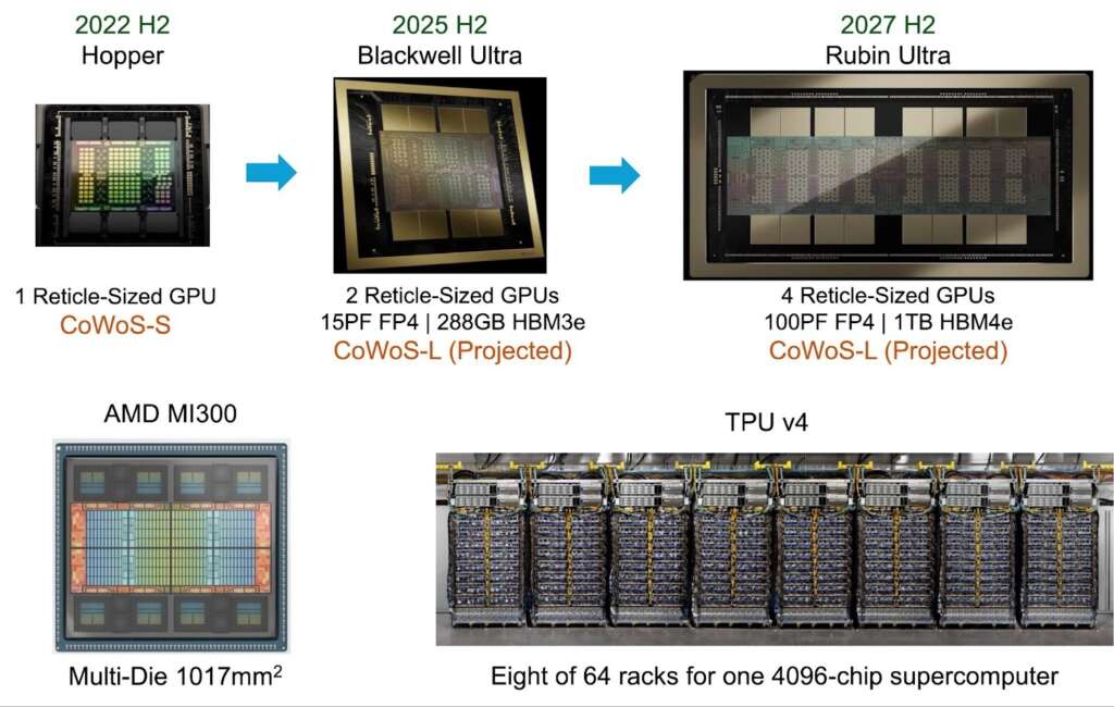
Figure.1: The trend toward larger and more complex chips [2][3][4][5][6]. This figure shows the progression from single-die to multi-die/chip by major vendors like NVIDIA, AMD, Google and others, who continue to expand chip size across generations.
Recent advances in semiconductor technology have made the vision of ever-larger chips increasingly practical. Improvements in advanced packaging, finer process nodes, and more effective cooling have enabled designs that were previously infeasible. Taiwan Semiconductor Manufacturing Company (TSMC), for example, has reported strong demand for wafer-scale integration technologies [7], which can scale chip sizes to a full wafer, often tens of times larger than conventional designs based on a single die (see Table 1).
For AI workloads, the advantages are clear. A full wafer can integrate millions of cores and tens of gigabytes of SRAM, interconnected through a network-on-chip. This architecture offers compute and memory bandwidth far beyond what even the largest chips today can provide (see Table 1), while keeping data movement local to the wafer.
Compared to conventional multi-chip systems, wafer-scale integration greatly reduces communication costs. Data transfer across the on-chip network is typically 10-100× more energy-efficient than board-level interconnects (see Table 1), enabling much tighter coupling of cores and memory. These efficiency gains have led organisations such as IEEE and TSMC to anticipate a coming wave of wafer-scale computers [7]. At the same time, AI companies, including Mxitral, Perplexity, Meta, and others, are beginning to explore wafer-scale systems as a platform for running advanced LLMs [8][9][10].
Table 1: System-on-Die vs. System-on-Wafer (Estimated on TSMC N3 Process Node). For metrics crucial to AI inference, like memory and inter-core communication bandwidth, system-on-wafer is about 100 to 1000 times more powerful than system-on-die.
| System-on-Die | System-on-Wafer | |
| Area | Typically 858 mm2 | Typically 73,062 mm2 |
| #Transistor (TSMC N3) | 1 trillion | ~10 trillion |
| Interconnect | PCB/RDL/SUB/WoW | Wafer |
| Die-to-die Efficiency | ~10s pJ/bit | ~0.1s pJ/bit |
| Die-to-die Bandwidth | ~1-10s TB/s | ~10 – 100s TB/s |
| Memory Bandwidth | 10s TB/s (crossbar) | 10s PB/s (aggregated via mesh) |
| Off-chip Memory | 10s – 100s GB HBM | 10s TB via TSMC SoW in 2027 |
How wafer-scale compute challenges software design
We want to understand how emerging wafer-scale computing challenges affect today’s AI system software design. Consider a commodity wafer-scale system such as the Cerebras WSE-2 (see Figure 2 [11]). These chips integrate hundreds of thousands of cores, each equipped with local fast memory, compute logic optimised for floating-point arithmetic, and a router that connects to other cores through a network-on-chip (NoC).
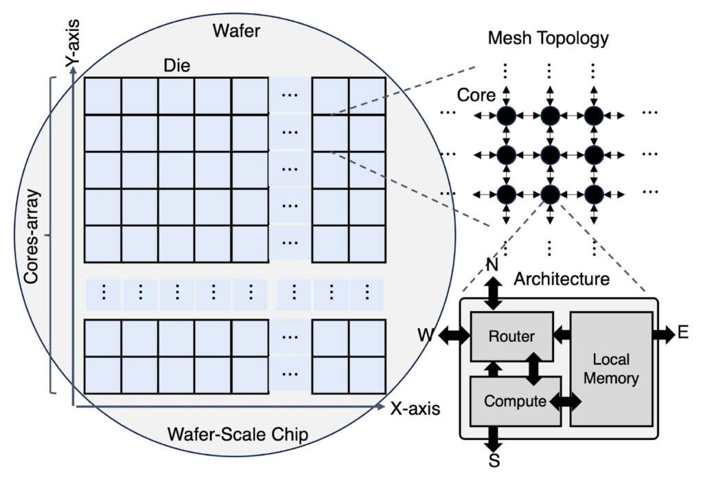
Figure 2: An example of a commodity wafer-scale AI system [9]. The wafer is composed of a massive array of cores, each with its own local memory, compute unit, and router. These cores are interconnected via a mesh network-on-chip, creating a highly parallel, distributed-memory architecture with unique software design challenges.
A key observation is that wafer-scale systems often expose their mesh-like interconnect to software developers (see Figure 2). Mesh interconnects are preferred because they simplify cooling and power delivery while offering cost-effective, near-linear communication scalability as core counts increase. A mesh topology also improves resilience against manufacturing defects. For example, Cerebras includes redundant links and cores across the wafer. When defective regions are detected, the hardware driver performs a hardware remapping process, reconfiguring the interconnect to bypass faulty areas and preserve a virtually intact two-dimensional mesh topology. This process effectively hides defects from developers, who can program the system as if it were built on an ideal, fully functional mesh network.
Another key observation is that wafer-scale systems adopt a distributed, asynchronous programming model. As core counts reach into the hundreds of thousands, maintaining a shared-memory abstraction becomes impractical, and global synchronisation quickly dominates execution time. Instead, wafer-scale systems rely on asynchronous message passing between cores. Each core executes independently, and developers can control how computation, data access, and message transmission occur asynchronously when handling incoming messages. Developers are also responsible for preventing potential deadlocks. Further, developers also need to define software-controlled data placement, deciding where data resides across the wafer and how it streams from the host to the chip during execution.
PLMR: A conceptual model to capture architectural traits
Programming a wafer-scale system demands careful attention to several key hardware architectural features; overlooking them can severely degrade software performance. We capture these in a conceptual device model, PLMR (pronounced “Plummer”), which identifies four characteristics that software developers must consider:
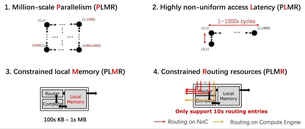
Figure 3: The PLMR model, which captures the key architectural traits of wafer-scale systems and outline the main challenges for software developers.
- Massive Parallelism (P): Leveraging the vast number of cores on a wafer requires sophisticated strategies for partitioning and replicating computation. Unlike traditional systems with tens or hundreds of GPUs, wafer-scale architectures may involve keeping millions of cores simultaneously active. This scale further demands careful scheduling to ensure that communication and computation are effectively overlapped across all cores.
- Highly Non-uniform Memory Access Latency (L): On a wafer-scale mesh, distance is a critical factor. When a core fetches data from a distant core’s memory, the request must traverse many intermediate routers. In an Nw × Nh 2D mesh, the worst-case distance is Nw + Nh hops, which, for a million-core wafer, can amount to several thousand hops. In practice, accessing remote memory can be roughly 1000× slower than accessing a core’s local memory. Minimising long-range communication is therefore essential for performance.
- Constrained per-core Local Memory (M): The large total on-chip memory of a wafer-scale system (tens of gigabytes) is, in fact, composed of many small fragments. Each core provides only a limited local memory, typically ranging from a few tens of kilobytes up to a few megabytes. This design choice reflects a tradeoff: smaller memories are faster and more energy-efficient, so wafer-scale architectures favour numerous small SRAM blocks over a few large ones. For software, the key implication is that all data, such as activations and weights, must be partitioned into chunks that fit within each core’s local store.
- Constrained Routing Resources (R): With millions of cores communicating, the on-chip network (NoC) becomes a critical and limited resource. Each core’s router has hardware constraints on the number of distinct routes it can maintain. For instance, on the Cerebras WSE-2, a router can recognise only a 5-bit address in message headers, allowing direct hardware addressing of at most 32 destinations. Sending to more destinations requires relaying messages through intermediate cores, which incurs additional software overhead for header parsing and rewriting. To mitigate these costs, communication patterns should favour locality; each core should primarily exchange data with a fixed set of neighbours, while global synchronisation and communication should be minimised.
When designing efficient software for wafer-scale compute, PLMR can serve as a checklist: performance-critical AI kernel and parallelism strategy should be PLMR-compliant. Importantly, PLMR is not limited to wafer-scale chips; it reflects a broader architectural shift from unified memory to large-scale NUMA designs. Unified memory, typically implemented with crossbars or all-to-all interconnects, scales poorly because networking cost grows exponentially with the number of cores and memory units. By contrast, emerging interconnects such as 2D mesh, ND mesh, 2D torus, and 3D torus scale with linear networking cost, but shift the complexity of maintaining efficient parallel computation onto software.
Software developers must now manage NUMA behaviour at scale, where memory access latency can differ substantially between nearby and distant cores. These programming challenges are already evident in non-wafer-scale architectures such as Tenstorrent and NVIDIA’s upcoming Rubin and Blackwell chips, where stream processor (SM) interconnects expose NUMA properties to developers, as well as in AI clusters organised around mesh-based topologies (e.g., Google TPU Pods and Tenstorrent Galaxy).
Limitations of today’s AI software design approaches
This brings us to a critical question: Are our AI software design approaches ready for wafer-scale compute? To run an AI model on a distributed memory architecture, existing works generally have two choices: (i) abstract the distributed local memory in each core as a shared memory and directly access data placed in a remote core through NoC; and (ii) explicitly partition computation into distributed cores and use message passing to exchange necessary data. We analyse two types of representative systems: AI runtimes or DNN compilers for shared memory architectures, such as GPUs (e.g., Ladder [12]); and compilers for distributed on-chip memory architectures (e.g., T10 [13] for GraphCore IPU).
Shared-memory AI systems. A shared-memory-based DNN compiler such as Ladder and others [14][15][16][12][18][19][20] usually assumes a uniform memory access pattern within the underlying memory hierarchy, which often focuses primarily on partitioning computation, with less emphasis on optimising data partitioning. However, as we described previously, a wafer-scale chip is formed by interconnecting a massive number of smaller cores via a mesh-like NoC. If one uses a shared-memory-based DNN compiler to create a uniform memory abstraction for the wafer-scale chip’s distributed on-chip memory, it will lead to severe long-distance and random communication between cores, and easily exceed the SRAM limits of a single core.
Distributed-memory AI systems. There are two main types of these methods: one is similar to T10 [13], designed for AI accelerators with an on-chip crossbar, which ensures a constant latency of memory access to any other cores on the same chip. The other is similar to AI parallel computing systems, such as Megatron-LM [17], which utilise tensor parallelism and pipeline parallelism, and are designed for high-performance clusters with full connectivity via NVLink, NVSwitch, and InfiniBand. However, crossbar and switch networks have limited scalability; an interconnection scale of millions would lead to severe cost overhead and cluster failure rates. The wafer-scale chip was designed with a mesh-like topology precisely for this reason. Therefore, existing work on distributed memory systems cannot be directly applied to wafer-scale chips either.
Harnessing wafer-scale compute for test-time scaling
The recent surge in interest in test-time scaling presents a compelling opportunity to demonstrate how wafer-scale computing can enable this emerging paradigm. The core idea of test-time scaling is simple: by allowing a Large Language Model (LLM) to “think longer”, that is, to generate significantly more tokens than in prior settings, the model can achieve much higher accuracy and robustness. This has been demonstrated in recent systems such as GPT-5, DeepSeek-R1, Gemini, and Claude 4.5.
The demand for test-time scaling creates strong pressure for ultra-low-latency decoding at the per-user level. A longer reasoning process can easily consume tens of thousands of tokens, and with the rise of agentic AI, the requirement may extend to millions of tokens per user. To keep this “thinking” process interactive, completing tasks within seconds rather than minutes, the system must decode tokens at under one millisecond, ideally approaching the microsecond level. Conventional AI chip designs cannot meet this requirement: their decoding throughput is fundamentally limited by HBM bandwidth, which typically supports only hundreds of tokens per second per user, insufficient for test-time scaling.
Wafer-scale systems, by contrast, provide orders of magnitude higher memory bandwidth. For example, the Cerebras WSE-2 chip delivers about 20 PB/s of aggregate bandwidth, representing the total sum of local memory bandwidth of its massive number of cores. This total sum far exceeds that of HBM, which sacrifices overall bandwidth for a unified memory design.
However, the advantage of high aggregate bandwidth does not come for free. The hardware relies on system software that must carefully coordinate asynchronous computation across all cores, using message passing to synchronise operations without deadlock, balance workloads, and avoid communication bottlenecks. Without such coordination, the system cannot fully realise the theoretical memory bandwidth that wafer-scale hardware promises.
Designing WaferLLM for efficient wafer-scale inference
Motivated by the above observation, we began developing WaferLLM two years ago. The results are particularly exciting. By redesigning the LLM inference software stack, aligning performance-critical AI kernels with parallelism strategies, we demonstrate, for the first time, that per-user LLM inference latency can be reduced to below one millisecond using today’s commodity wafer-scale technology. We present the full details of WaferLLM in our OSDI 2025 paper [11]. In the following sections, we briefly highlight several key design principles of WaferLLM.
At a high level, WaferLLM takes LLM checkpoints and applies new strategies to parallelise their execution across wafer cores. These strategies target two critical inference stages: prefill and decode (see Figure 4). The prefill stage involves loading the model weights, with its performance dominated by General Matrix-Matrix Multiplication (GEMM). The decode stage requires loading both the model weights and the KV-cache, where the performance-critical operation is General Matrix-Vector Multiplication (GEMV).
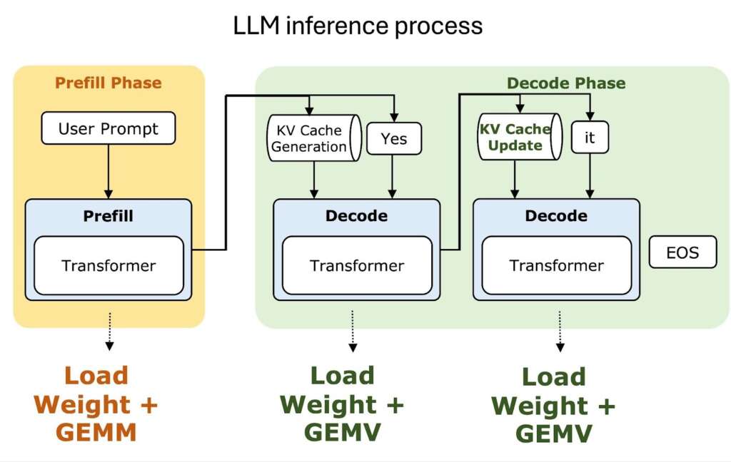
Figure 4: The two key stages of LLM inference, Prefill and Decode. Effective test-time scaling depends on scaling LLM decoding performance for each user.
Wafer-scale-friendly parallelism strategies. First, for parallelisation, WaferLLM partitions activation and weight matrices along two dimensions during prefill, and replicates while partitioning activation vectors during decode. This design aligns with the wafer’s massive parallelism and ensures compliance with the P and M requirements in PLMR.
Second, WaferLLM avoids costly matrix and vector transpositions, which are common pitfalls in wafer-scale computing and violate the L in PLMR. Instead, it uses transpose-aware GEMM algorithms and pre-transposed parameter placement.
Boosting the performance of key parallel compute operations. For GEMM and GEMV, WaferLLM introduces PLMR-compliant algorithms tailored to mesh interconnects, called MeshGEMM and MeshGEMV. These algorithms are explicitly designed to align with the constraints of the PLMR model and deliver highly efficient performance on wafer-scale systems.
As shown in Figure 5(a), MeshGEMM addresses the Latency (L) and Routing (R) challenges by using cyclic shifting and interleaving to construct the shortest possible communication paths. Compared with state-of-the-art GEMM algorithms optimised for Clos or Torus topologies, MeshGEMM reduces communication overhead by 2-5× on mesh networks, leading to 1.3-2× end-to-end GEMM speedups.
For MeshGEMV, illustrated in Figure 5(b), WaferLLM employs a K-tree Allreduce to minimise the length of critical communication paths. On mesh topologies, MeshGEMV reduces communication overhead by 1.5-6× compared with GPU-cluster GEMV algorithms, and achieves 2.5-3× faster performance.
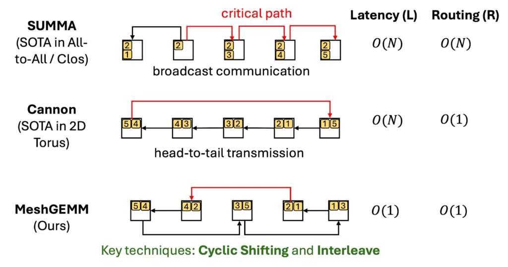
Figure 5(a): GEMM Communication Comparison on mesh network. MeshGEMM uses Cyclic-shifting and Interleave to reduce communication latency from O(N) to O(1) compared to standard algorithms.
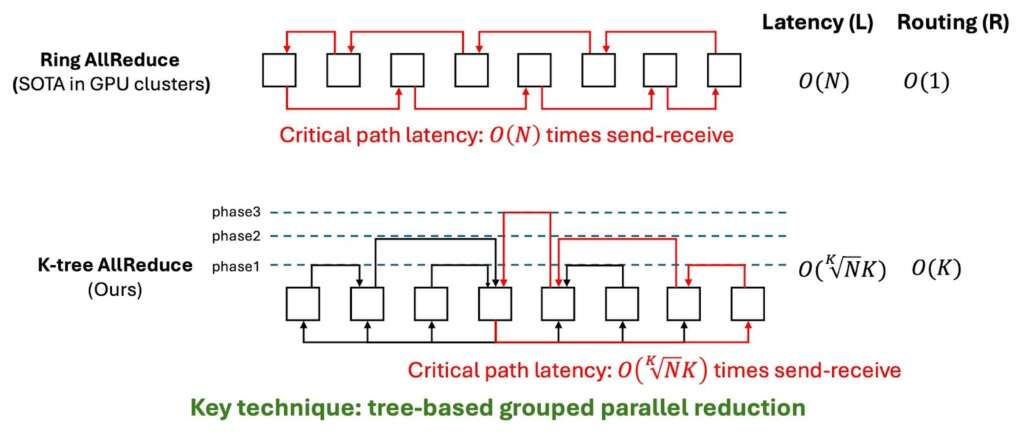
Figure 5(b): GEMV Communication Comparison on mesh network. MeshGEMV employs a K-tree Allreduce to shorten the critical communication path latency.
Another key operation is KV cache management. For this, WaferLLM introduces a novel shift-based KV-cache management algorithm that incrementally redistributes cache entries across adjacent cores in parallel. This design aligns with the Constrained Local Memory (M) principle of PLMR, ensuring balanced memory utilisation and consistent workload distribution across the wafer. As a result, it extends the maximum inference length by several hundred times compared to baseline systems and eliminates out-of-memory errors.
Scaling efficiency: wafer-scale vs. multi-chip approaches
With WaferLLM, we are now able to fully utilise a wafer-scale chip. The next question is whether wafer-scale computing truly fulfils its promise of providing more efficient scaling than today’s approaches, which coordinate multiple chips interconnected by high-speed networks such as NVLink and InfiniBand.
We evaluated WaferLLM on a real Cerebras WSE-2 wafer-scale chip (TSMC 7nm) against state-of-the-art GPU-based inference systems, including SGLang and vLLM, deployed on NVIDIA A100 GPUs (also TSMC 7nm) interconnected via NVLink and InfiniBand.
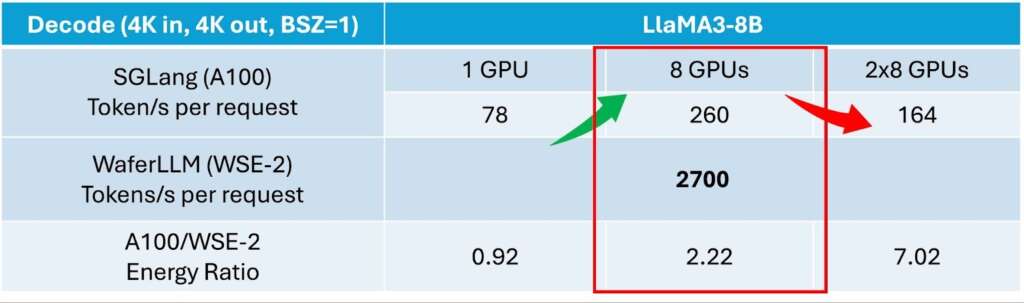
Figure 6: Scaling efficiency comparison for wafer-scale and multi-GPU systems. For LlaMA3-8B decoding, the wafer-scale system (WSE-2) achieves 2,700 tokens/s, significantly outperforming an 8-GPU A100 server (260 tokens/s). The world-record results highlight the wafer-scale system’s superior performance and its improved energy efficiency at scale, avoiding the communication bottlenecks of multi-chip setups.
As shown in Figure 6, when the number of GPUs increases from one to eight through tensor parallelism, decoding throughput rises from 78 to 260 tokens per second. While this improvement is substantial, it falls short of ideal 8× scaling, reflecting NVLink’s communication overheads that affect decode latency, a key metric for test-time compute. Performance further declines when scaling beyond a single server: moving from 8 to 16 GPUs introduces InfiniBand overheads that reduce throughput.
In comparison, WaferLLM achieves 2,700 tokens per second, corresponding to sub-millisecond latency per decoded token. This level of performance enables real-time AI agent applications that are currently difficult to support on conventional clusters.
Beyond performance, we also examine whether wafer-scale systems can achieve efficient test-time scaling, higher performance without disproportionate energy costs. Normalising decoding throughput by power draw (A100 GPU vs. Cerebras WSE-2), WaferLLM shows an energy ratio of 0.92 compared to SGLang on a single A100 (values below one indicate higher efficiency for the A100). However, when scaling to 8 GPUs, the ratio exceeds one and reaches 2.22, indicating that wafer-scale systems become more energy-efficient as scale increases.
It is worth noting that the wafer-scale results remain preliminary, as runtime, core, and on-chip interconnect efficiency are still being optimised. Continued improvements in the software stack are expected to enhance both performance and efficiency.
Rethinking the full AI system stack for wafer-scale compute
WaferLLM has demonstrated the strong potential of wafer-scale AI systems. Yet, realising the full promise of wafer-scale computing requires rethinking the entire AI stack, from model architectures to software systems and hardware design.
Aligning AI model designs with wafer-scale compute.
A first step is to adapt model architectures to the unique strengths of wafer-scale systems. Wafer-scale hardware offers massive parallelism and unprecedented on-chip bandwidth. This raises a critical question: should future model architectures and training algorithms be explicitly designed for wafer-scale platforms? For example, given a fixed parameter budget, should models become wider, with larger hidden dimensions, or deeper, with more layers? Addressing this requires careful study of how model structure interacts with bandwidth utilisation and parallelism at the wafer scale. Tailoring models to these characteristics could unlock significant gains in both performance and efficiency.
Advancing wafer-scale software capabilities.
Wafer-scale’s extreme parallelism and distributed memory architecture also call for rethinking system software. Traditional stacks, designed for off-chip scaling and relatively uniform memory access, may prove inadequate for this purpose. Managing distributed memory and scheduling fine-grained tasks across millions of cores introduces challenges that could require new memory management and parallel compute systems, runtimes, and schedulers. Even long-standing programming models such as MPI, originally created for clusters, may need to be revisited. A wafer-native distributed programming paradigm could simplify development, improve performance, and better exploit locality and parallelism inherent to wafer-scale hardware.
Looking ahead, future wafer-scale AI computers will integrate even greater memory capacity, enabling large numbers of concurrent users to share the same machine. This raises a fundamental question: how should an operating system be designed to manage such massive systems? Unlike conventional designs, where memory and cores are organized in a unified shared space, a wafer-scale operating system must coordinate vastly larger pools of compute, memory, and I/O resources in a distributed and asynchronous manner—even though they reside on a single chip. This shift will transform core OS mechanisms for resource abstraction, concurrency, fairness, debugging, and beyond.
Designing more efficient wafer-scale hardware.
Ultimately, there are opportunities for future hardware innovations that extend beyond today’s mesh topologies. While mesh architectures offer strong simplicity in both manufacturing and programming, they are not always optimal for operations such as all-reduce communications, which are common in attention-based models. Can we design specialised NoC topologies that preserve scalability to millions of cores while accelerating such communication patterns? Exploring these directions may further amplify the efficiency and performance advantages of wafer-scale systems.
References
[1] Wei, J., Tay, Y., Bommasani, R., Raffel, C., Zoph, B., Borgeaud, S., Yogatama, D., Bosma, M., Zhou, D., Metzler, D., Chi, E. H., Hashimoto, T., Vinyals, O., Liang, P., Dean, J., & Fedus, W. “Emergent Abilities of Large Language Models,” Transactions on Machine Learning Research (2022).
[2] Andersch, M., Palmer, G., Krashinsky, R., Stam, N., Mehta, V., Brito, G., & Ramaswamy, S. “NVIDIA Hopper Architecture In-Depth,” NVIDIA Technical Blog, March 22, 2022. https://developer.nvidia.com/blog/nvidia-hopper-architecture-in-depth/.
[3] NVIDIA. “NVIDIA Blackwell Architecture — The Engine Behind AI Factories,” 2025. https://www.nvidia.com/en-us/data-center/technologies/blackwell-architec….
[4] NVIDIA Writers. “GTC 2025 — Announcements and Live Updates,” NVIDIA Blog, March 25, 2025. https://blogs.nvidia.com/blog/nvidia-keynote-at-gtc-2025-ai-news-live-up….
[5] AMD. AMD Instinct™ MI325X Accelerators. https://www.amd.com/en/products/accelerators/instinct/mi300/mi325x.html.
[6] Jouppi, N., Kurian, G., Li, S., Ma, P., Nagarajan, R., Nai, L., Patil, N., Subramanian, S., Swing, A., Towles, B., et al. “Tpu v4: An optically reconfigurable supercomputer for machine learning with hardware support for embeddings,” Proceedings of the 50th annual international symposium on computer architecture (2023), pp. 1–14.
[7] LaPedus, M. “TSMC bets big on advanced packaging,” 2023. https://spectrum.ieee.org/tsmc-advanced-packaging.
[8] Cerebras Systems. “Cerebras Powers Perplexity Sonar with Industry’s Fastest AI Inference,” 2025. https://www.cerebras.ai/press-release/cerebras-powers-perplexity-sonar-w….
[9] Wang, J. “Cerebras Brings Instant Inference to Mistral Le Chat,” 2025. https://cerebras.ai/blog/mistral-le-chat.
[10] Cerebras Systems. “Cerebras and G42 Break Ground on Condor Galaxy 3, an 8 exaFLOPs AI Supercomputer,” 2024. https://cerebras.ai/press-release/cerebras-g42-announce-condor-galaxy-3.
[11] He, C., Huang, Y., Mu, P., Miao, Z., Xue, J., Ma, L., Yang, F., & Mai, L. “WaferLLM: Large Language Model Inference at Wafer Scale,” 19th USENIX Symposium on Operating Systems Design and Implementation (OSDI 25) (2025), pp. 257–273.
[12] Wang, L., Ma, L., Cao, S., Zhang, Q., Xue, J., Shi, Y., Zheng, N., Miao, Z., Yang, F., Cao, T., et al. “Ladder: Enabling Efficient Low-Precision Deep Learning Computing through Hardware-aware Tensor Transformation,” 18th USENIX Symposium on Operating Systems Design and Implementation (OSDI 24) (2024), pp. 307–323.
[13] Liu, Y., Xue, Y., Cheng, Y., Ma, L., Miao, Z., Xue, J., & Huang, J. “Scaling Deep Learning Computation over the Inter-Core Connected Intelligence Processor with T10,” Proceedings of the ACM SIGOPS 30th Symposium on Operating Systems Principles (2024), pp. 505–521.
[14] Chen, T., et al. “TVM: An Automated End-to-End Optimization Stack for Deep Learning,” SSP 2018 (2018).
[15] Ma, L., Xie, Z., Yang, Z., Xue, J., Miao, Y., Cui, W., Hu, W., Yang, F., Zhang, L., & Zhou, L. “Rammer: Enabling Holistic Deep Learning Compiler Optimizations with rTasks,” 14th USENIX Symposium on Operating Systems Design and Implementation (OSDI 20) (2020), pp. 881–897.
[16] Shi, Y., Yang, Z., Xue, J., Ma, L., Xia, Y., Miao, Z., Guo, Y., Yang, F., & Zhou, L. “Welder: Scheduling Deep Learning Memory Access via Tile-graph,” 17th USENIX Symposium on Operating Systems Design and Implementation (OSDI 23) (2023), pp. 701–718.
[17] Narayanan, D., Shoeybi, M., Casper, J., LeGresley, P., Patwary, M., Korthikanti, V., Vainbrand, D., Kashinkunti, P., Bernauer, J., Catanzaro, B., Phanishayee, A., & Zaharia, M. “Efficient large-scale language model training on GPU clusters using Megatron-LM,” Proceedings of the International Conference for High Performance Computing, Networking, Storage and Analysis (2021), pp. 1–15.
[18] Zhao, Y., et al. “Ansor: A Compiler Stack for Auto-Tuning Tensor Programs,” IEEE Transactions on Software Engineering (2020).
[19] Zheng, S., Liang, Y., Wang, S., Chen, R., & Sheng, K. “FlexTensor: An Automatic Schedule Exploration and Optimization Framework for Tensor Computation on Heterogeneous System,” Proceedings of the Twenty-Fifth International Conference on Architectural Support for Programming Languages and Operating Systems (2020), pp. 859–873.
[20] Zhu, H., Wu, R., Diao, Y., Ke, S., Li, H., Zhang, C., Xue, J., Ma, L., Xia, Y., Cui, W., Yang, F., Yang, M., Zhou, L., Cidon, A., & Pekhimenko, G. “ROLLER: Fast and Efficient Tensor Compilation for Deep Learning,” 16th USENIX Symposium on Operating Systems Design and Implementation (OSDI 22) (2022), pp. 233–248.